DS1722
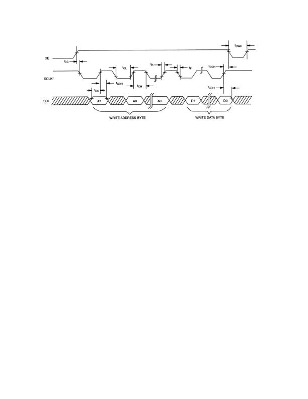
TIMING DIAGRAM: SPI WRITE DATA TRANSFER Figure 12
*SCLK can be either polarity, timing shown for CPOL = 1.
NOTES:
1. All voltages are referenced to ground.
2. Logic 0 voltages are specified at a sink current of 3 mA.
3. Logic 1 voltages are specified at a source current of 1 mA.
4. I
13 of 14
CC
specified with SCLK=V and CE=GND. Typical I is 0.25 礎 and I
DDD
CC1
CC
is 0.3 mA at 25癈
and V
DDD =
2.65V
.
5. Measured at V =0.7 V or V
IH
DDD
IL
=0.2 V and 10 ms maximum rise and fall time.
DDD
6. Measured with 50 pF load
7. Measured at V =0.7 V or V
OH
DDD
OL
=0.2 V . Measured from the 50% point of SCLK to the V
DDD
OH
minimum of SDO.
发布紧急采购,3分钟左右您将得到回复。
相关PDF资料
DS1775R7+T&R
IC THERMOM/STAT DIG 111 SOT-23-5
DS1821C+
IC THERMOMETER/STAT PROG 3-TO92
DS1825U+T&R
IC THERMOMETER DIGITAL 8-USOP
DS1842N+T&R
IC CURRENT MONITOR 14TDFN
DS18B20+PAR
IC THERM MICROLAN PROG-RES TO-92
DS18B20Z/T&R
IC THERM MICROLAN PROG-RES 8SOIC
DS2740U+T&R
IC CURRENT GAUGE(15BIT) 8UMAX
DS28EA00U+T&R
IC THERMOMETER 1-WIRE 8-USOP
相关代理商/技术参数
DS1722S/T&R
制造商:Maxim Integrated Products 功能描述:SPI 3-WIRE THERMOMETER SOIC T&R - Tape and Reel 制造商:Maxim Integrated Products 功能描述:IC THERMOMETER DIG 3-WIRE 8-SOIC
DS1722S/T&R
功能描述:板上安装温度传感器 RoHS:否 制造商:Omron Electronics 输出类型:Digital 配置: 准确性:+/- 1.5 C, +/- 3 C 温度阈值: 数字输出 - 总线接口:2-Wire, I2C, SMBus 电源电压-最大:5.5 V 电源电压-最小:4.5 V 最大工作温度:+ 50 C 最小工作温度:0 C 关闭: 安装风格: 封装 / 箱体: 设备功能:Temperature and Humidity Sensor
DS1722S+
功能描述:板上安装温度传感器 Digital Thermometer & Thermostat RoHS:否 制造商:Omron Electronics 输出类型:Digital 配置: 准确性:+/- 1.5 C, +/- 3 C 温度阈值: 数字输出 - 总线接口:2-Wire, I2C, SMBus 电源电压-最大:5.5 V 电源电压-最小:4.5 V 最大工作温度:+ 50 C 最小工作温度:0 C 关闭: 安装风格: 封装 / 箱体: 设备功能:Temperature and Humidity Sensor
DS1722S+T&R
制造商:Maxim Integrated Products 功能描述: 制造商:Maxim Integrated Products 功能描述:TEMP SENSOR DGTL 3-WIRE/SPI 8SOIC - Tape and Reel 制造商:Maxim Integrated Products 功能描述:IC THERMOMETER DIG 3-WIRE 8-SOIC
DS1722S+T&R
功能描述:板上安装温度传感器 Digital Thermometer & Thermostat RoHS:否 制造商:Omron Electronics 输出类型:Digital 配置: 准确性:+/- 1.5 C, +/- 3 C 温度阈值: 数字输出 - 总线接口:2-Wire, I2C, SMBus 电源电压-最大:5.5 V 电源电压-最小:4.5 V 最大工作温度:+ 50 C 最小工作温度:0 C 关闭: 安装风格: 封装 / 箱体: 设备功能:Temperature and Humidity Sensor
DS1722U
功能描述:板上安装温度传感器 RoHS:否 制造商:Omron Electronics 输出类型:Digital 配置: 准确性:+/- 1.5 C, +/- 3 C 温度阈值: 数字输出 - 总线接口:2-Wire, I2C, SMBus 电源电压-最大:5.5 V 电源电压-最小:4.5 V 最大工作温度:+ 50 C 最小工作温度:0 C 关闭: 安装风格: 封装 / 箱体: 设备功能:Temperature and Humidity Sensor
DS1722U/T&R
制造商:Maxim Integrated Products 功能描述:THE MAXIM DS1722U/T&R IS A TEMPERATURE SENSOR. - Tape and Reel 制造商:Maxim Integrated Products 功能描述:Maxim DS1722U/T&R, Digital Thermometer and thermostat -55C to +125C 2.65V-5.5V 8-pin uMAX 制造商:Maxim Integrated Products 功能描述:IC THERMOMETER DIG 3-WIRE 8-USOP
DS1722U/T&R
功能描述:板上安装温度传感器 RoHS:否 制造商:Omron Electronics 输出类型:Digital 配置: 准确性:+/- 1.5 C, +/- 3 C 温度阈值: 数字输出 - 总线接口:2-Wire, I2C, SMBus 电源电压-最大:5.5 V 电源电压-最小:4.5 V 最大工作温度:+ 50 C 最小工作温度:0 C 关闭: 安装风格: 封装 / 箱体: 设备功能:Temperature and Humidity Sensor